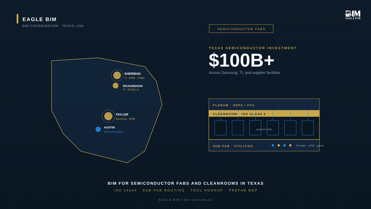
Texas is in the middle of the largest semiconductor manufacturing buildout in American history, and most of the construction industry has not caught up. Samsung’s Taylor fab is a $44 billion project on 1,200 acres outside Austin, with first light expected this year and Tesla on the books for $16.5 billion of AI chip business through 2033. Samsung Taylor BIM scope work alone is generating coordination demand at a scale very few firms can fulfill. Texas Instruments just opened SM1 in Sherman, the first of four planned fabs that together will deliver 1.4 million square feet of cleanroom space when complete. TI is investing more than $60 billion across seven fabs, mostly in Texas. Combine these with TI’s Richardson facilities, Samsung’s legacy Austin campus, and a long line of supplier facilities being built to feed the majors, and you get a market that needs BIM for semiconductor fabs at a level very few firms have actually delivered.
This blog is for the contractors, MEP subs, and owner’s reps trying to figure out what makes a fab build different from anything else they’ve worked on. It walks through cleanroom classifications, why the sub-fab is harder than the cleanroom most people are looking at, what specialty utilities the model has to carry, and how prefab actually works on a fab project. By the end you’ll know what fab MEP coordination requires, why ISO 14644 shows up in every BEP for these builds, and what to ask a BIM partner before you let them anywhere near a tool hookup. Strong cleanroom BIM work is what separates teams that have done this before from teams that are about to learn the hard way.
Everything that follows is shaped by what’s actually being built right now in Texas. This is not a generic explainer about cleanrooms. It’s a working contractor’s view of the buildings reshaping the state economy. Whether the project is Samsung Taylor BIM scope, a TI Sherman supplier facility, or one of the dozens of packaging and equipment buildings going up around Austin, the same fundamentals apply. Get the cleanroom BIM right at the design stage, get the sub-fab routing coordinated at LOD 400, and the rest of the project has a fighting chance to land on schedule.
Why the Texas Semiconductor Boom Is Reshaping Construction
Three things are happening at once. Federal CHIPS Act funding is flowing into Texas at a scale nobody planned for. Customer demand for advanced chips, especially for AI training, has become the single biggest pull on the global manufacturing pipeline. And Texas has the land, power, and regulatory speed to actually absorb the buildout, which most other states do not.
Samsung’s $44 billion Taylor fab is the headline. The original $17 billion plan from 2021 has more than doubled in scope, and Samsung’s Austin campus continues to operate alongside it. Texas Instruments is building a $40 billion, four-fab mega-site in Sherman, with SM1 already in production and SM2’s exterior shell already up. Add RFAB1 (the world’s first 300mm analog fab when it opened in 2011) and RFAB2 in Richardson, the Soulbrain TX phosphoric acid facility supplying Samsung, and the dozen other supplier and packaging facilities being announced in the same corridor, and semiconductor construction Texas is now a multi-decade pipeline.
If you want a sense of what’s in the queue, the SEMI industry association keeps the most current view of fab announcements globally. The Texas projects show up disproportionately in any 2026 forecast, and the supplier ecosystem feeding Samsung Taylor, TI Sherman, and the Richardson sites is itself generating thousands of jobs and millions of square feet of construction.
What this means for the construction industry is that fab work is no longer a niche. It’s a major segment of Texas commercial construction for the next decade, and the firms that figure out BIM for semiconductor fabs now will be the ones bidding on the next wave of supplier and packaging facilities behind the majors.
What Makes a Fab the Most Complex Build in the Country
Fabs are uniquely difficult buildings. The MEP density is higher than a hospital. The vibration tolerances are tighter than anything outside specialized research labs. The contamination control protocols turn ordinary construction sequences into elaborate dance routines. And the equipment that finally goes inside the building is some of the most expensive industrial hardware on Earth, which means every dimension and every clearance has to land within tolerances most contractors have never had to work to.
Cleanroom Classifications and ISO 14644
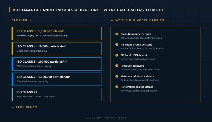
ISO 14644 sets the rules for how clean a cleanroom has to be. The classifications run from ISO Class 1 (theoretical, basically lab-only) down through ISO Class 9. A modern semiconductor fab cleanroom typically operates at ISO Class 3, 4, or 5 depending on the process step. Photolithography areas, where EUV scanners are doing sub-3-nanometer patterning, demand the cleanest space. Wafer transport corridors and tool staging operate at slightly relaxed levels. The BIM model has to carry every one of these zones as discrete spaces with their own boundary conditions. Solid ISO 14644 cleanroom modeling at this stage is what enables every downstream coordination decision.
ISO 14644 cleanroom modeling is not just about marking which room is which class. The model has to capture air change rates per zone (often 300+ ACH for the cleanest spaces), HEPA and FFU layout density, pressure cascades between adjacent rooms, particle-control material specifications for every surface, and penetration sealing details for every wall, ceiling, and floor pass-through. Get any of this wrong in the model and you get a cleanroom that can’t hit its certification when commissioning starts. This is where good cleanroom BIM work pays for itself many times over, because the alternative is a recommissioning cycle that delays first wafer.
Eagle BIM’s ISO 14644 cleanroom modeling approach treats every classified zone as a discrete coordination space with its own material schedule, air system requirements, and pressure relationship to adjacent zones. The federated model carries all of that data, which means architectural, mechanical, and structural changes can be tested against classification requirements before they become field problems.
Vibration Isolation and Structural Sensitivity
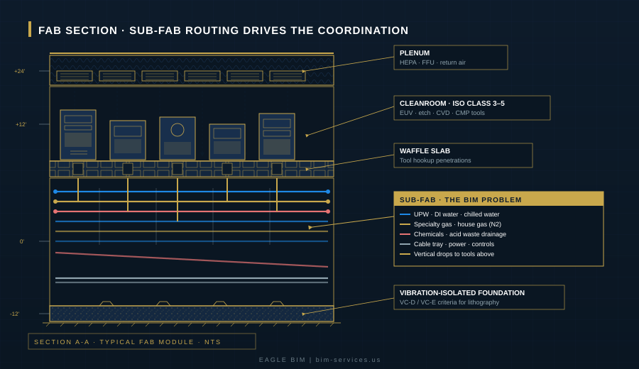
Lithography tools, especially the EUV scanners Samsung is bringing online at Taylor, need stability measured in nanometers. The building has to be designed to keep vibration below VC-D or VC-E levels in the most sensitive bays. That means thick concrete, isolated foundations, often pneumatic or hydraulic mounts under specific tools, and very careful coordination with anything else in the building that moves or generates resonance.
Structural BIM for a fab gets unusual. You’re modeling waffle slabs that the cleanroom sits on, with thousands of penetrations cut precisely so utility drops can pass through to the tools above. You’re modeling the sub-fab structural floor that has to carry the weight of pumps, abatement systems, and water treatment skids. And you’re coordinating all of that with the vibration isolation strategy, because a structural connection in the wrong place can transmit machine vibration directly into the lithography deck.
Sub-Fab Utility Routing
This is the part most BIM teams underestimate. Below the cleanroom floor sits the sub-fab, a service level dense with piping, ducting, cable, and equipment. Every tool on the cleanroom floor has utility connections that drop through the waffle slab into the sub-fab. Multiply that by hundreds of tools, and the sub-fab becomes the most coordination-intensive single space in the building.
Sub-fab routing has to handle ultrapure water (UPW), de-ionized water, multiple specialty gas lines, process chemicals, vacuum lines, compressed air, chilled water, acid waste drainage, and the full electrical feed for every tool. All of this lives in the same space. The pipes can’t share supports if they carry incompatible fluids. The drainage has to slope correctly. The gas lines need leak detection. The waste lines need chemical-resistant materials. The electrical feeds need separation from anything that could create induced currents. None of this fits in the field. It has to be modeled to LOD 400 before fabrication starts.
Tool Hookup and Equipment Integration
Each process tool in a fab has its own hookup specification. The vendor sends a document with utility connection points, dimensions, weight, vibration limits, exhaust requirements, and clearance envelopes. The BIM team has to build that vendor model into the federated coordination model and verify that every hookup point matches the routing coming from the sub-fab. If the tool hookup spec changes (and they do change, often during fabrication), the model has to update and the sub-fab routing has to verify.
Tool-in is the moment of truth. A new lithography tool weighs tens of thousands of pounds, gets craned in through a roof opening, set on its isolation mount, and connected to dozens of utilities. If the BIM model said the connection points were six inches to the left of where they actually are, the install crew finds out at the worst possible moment. BIM for semiconductor fabs exists to make sure that doesn’t happen. On Samsung Taylor BIM scope work, every tool hookup gets verified against the ISO 14644 cleanroom modeling data and the sub-fab routing before any vendor tool ships to site, because the cost of a mismatched connection is measured in weeks of schedule slippage.
Why BIM Is Non-Negotiable on Fab Projects
Some construction work can be planned with 2D drawings and field judgment. Fab work cannot. The system density alone makes traditional coordination impossible, and that’s before you add the cleanliness requirements, vibration constraints, and tool hookup complexity. BIM for semiconductor fabs is mandatory on every Tier 1 project, and the BEPs that come out of Samsung, TI, and TSMC’s Texas operations all spec it that way. Samsung Taylor BIM requirements alone set a benchmark that suppliers and adjacent projects then inherit, and ISO 14644 cleanroom modeling requirements show up in every one of those BEPs.
System Density Beyond Hospital MEP
A hospital is a dense MEP building. A fab is denser. The sub-fab alone often has more piping per linear foot than an entire hospital basement. Add the cleanroom plenum above, the waffle slab in between, the structural members weaving through both, and you have a building where every cubic foot of space is competing among multiple disciplines. The federated model has to resolve all of it before construction starts because there’s no slack in the field to figure it out later.
On a recent Samsung Taylor BIM scope (or any project at that scale), the federated model carries architectural, structural, mechanical, electrical, plumbing, fire protection, low-voltage, process piping, specialty gas, UPW, chemical distribution, acid waste, vacuum, controls, and tool hookup as separate disciplines. That’s 14 plus disciplines competing for space, and every one of them has to coordinate at LOD 400 before fabrication. Fab MEP coordination at this level is fundamentally different from anything in standard commercial work, and the Samsung Taylor BIM benchmark is now what other semiconductor construction Texas projects are being measured against.
Cleanroom BIM at this density requires modeling tools the standard commercial workflow does not use. Specialty piping families, vendor tool models, vibration zones, classification boundaries, and material schedules per zone all live inside the federated model. Coordinating all of that takes a team that has done it before, which is one reason semiconductor construction Texas work tends to flow to a small number of specialized firms.
Specialty Gas, Process Water, and Chemical Distribution
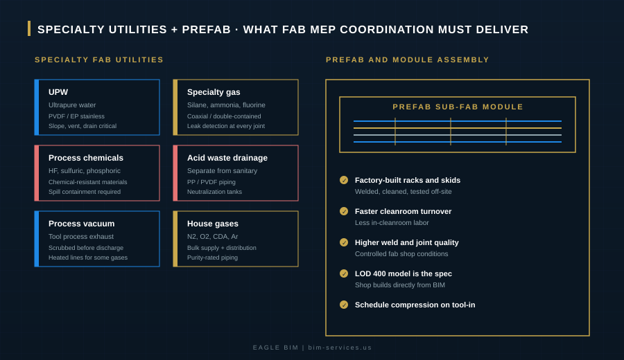
This is where fab MEP coordination diverges sharply from anything in commercial construction. Specialty gases include silane, ammonia, fluorine, chlorine, and other materials that range from pyrophoric to corrosive to acutely toxic. The piping is often coaxial or double-contained, with leak detection at every joint. Routing has to keep these lines away from anything that could start a fire or create a contamination event. The materials specification is dictated by the fluid (PVDF for some, electropolished stainless for others, special alloys for the most reactive).
Process water is its own discipline. Ultrapure water has to maintain resistivity values that ordinary plumbing can’t preserve. Slope, dead-leg avoidance, vent placement, and material selection all matter. Acid waste drainage runs in completely separate piping from sanitary, with its own neutralization tanks and chemical-resistant materials. The model has to keep all of this organized, and the fab MEP coordination team has to know which fluid lives in which line, because mixing them up in a clash report is how you get a deeply unsafe building.
Vibration and Acoustic Coordination
Vibration coordination is mostly a structural and equipment problem, but it shows up in BIM too. The model has to identify which spaces are vibration-sensitive, what the maximum allowable vibration levels are, and what equipment is generating significant vibration that needs to be isolated or relocated. Pumps, compressors, vacuum equipment, and air handlers all become things you can’t just place wherever there’s room. The coordination model is where these constraints get reconciled.
Acoustic coordination follows similar logic. Some process tools are acoustically sensitive. Some generate acoustic energy that interferes with adjacent operations. The BIM team has to flag both, and the architectural and structural teams have to design around them. Ignoring this until commissioning is a great way to learn an expensive lesson. Good cleanroom BIM work treats acoustic and vibration zones as first-class data in the federated model, not afterthoughts.
| Building a Fab in Texas? Eagle BIM Coordinates Across Every Discipline.
We model architectural, structural, MEP, specialty gas, UPW, chemical, process vacuum, and tool hookup at LOD 400 for semiconductor construction Texas projects. Cleanroom-first workflow, sub-fab focus, prefab-ready deliverables. Built for the way fabs actually go up. |
Coordination Challenges Specific to Texas Fab Sites
Beyond the universal fab challenges, Texas adds its own layer of complexity. The climate, the grid, the available water, and the local code interpretation all shape how a fab gets built here versus how the same project would get built in Arizona or upstate New York. BIM for semiconductor fabs in Texas means understanding these regional realities and modeling for them, not just copying a template from another market. Semiconductor construction Texas is a distinct market with its own permitting timelines, its own ERCOT power dynamics, and its own water availability constraints, all of which feed back into the BIM model.
Climate and HVAC Load
A cleanroom is essentially a giant HVAC system with a building wrapped around it. The number of air changes per hour, the filtration stages, the cooling load to keep tools at their target temperatures, the dehumidification load, and the make-up air all stack up to enormous mechanical capacity. In Texas, the outside design conditions push every one of these numbers up. A fab in Taylor sees 100-degree-plus ambient temperatures for months on end, and the cooling design has to handle that without losing classification.
This drives the sizing of chillers, cooling towers, and air handling units far above what a similar fab would need in a temperate climate. The BIM model has to capture all of this equipment, the chilled water piping serving it, the makeup air pathways, and the integration with the cleanroom air return system. None of it is academic. Get the cooling capacity wrong on a Texas fab and you can’t make chips during summer.
Power Infrastructure and Substation Integration
A modern hyperscale fab can pull as much power as a small city. Samsung Taylor draws hundreds of megawatts, and the substation that feeds it is itself a significant construction project. Power infrastructure for a fab includes the utility interconnect, on-site substations, transformers, switchgear lineups, UPS systems sized for the most sensitive loads, generators for backup, and the distribution network running through the building.
The BIM model integrates all of this with the rest of the federated coordination model. Substation yards have their own clearance requirements (often dictated by NESC rather than NEC), and the routing from substation to building service entrance to internal distribution gets coordinated against architectural, structural, and other MEP routing. ERCOT interconnection planning happens in parallel, and the construction sequence has to land power at the building before tool installation can begin. Fab MEP coordination that ignores the substation integration is incomplete.
Prefabrication and Module Assembly for Fab MEP
Speed-to-tool is the metric on a fab project. From the first concrete pour to first wafer out, the timeline is typically 30 to 36 months for a major fab build. Compressing that schedule directly affects how soon the operator can start producing chips, which directly affects revenue. Prefab and modular assembly are how that compression happens.
On the sub-fab side, MEP modules get built in a fab shop and shipped to site as complete units. Pipe racks with all process water, chemical, and gas lines pre-installed. Electrical skids with switchgear and distribution preassembled. Acid waste neutralization modules. UPW polishing skids. Each module gets built from the LOD 400 BIM model, tested in the shop, then bolted and connected on site. The sub-fab routing work that would have taken weeks of in-place welding gets compressed into days of module placement and final connections.
On the cleanroom side, prefab is more limited because of contamination control, but partition systems, ceiling grid, and FFU modules all show up pre-engineered. Even some tool hookup points are now being prefabricated as drop-in assemblies. The common thread across all of it is that the BIM model has to be accurate at LOD 400 before anything goes to the prefab shop. A modeling error becomes a fabrication error becomes a field rework problem, and on a fab project there’s no time to absorb that.
Eagle BIM’s prefab workflow on a fab project starts with a federated LOD 400 model six to ten weeks before the fab shop needs each module. We run shop-level QC on every module model before it goes to fabrication. Field-verified updates flow back into the model continuously during install so the planned-vs-actual delta stays visible. That tight loop is what keeps a fab schedule on track when one tool delivery slips by three weeks and the whole sequence has to flex. Samsung Taylor BIM scope work, TI Sherman supplier facilities, and other semiconductor construction Texas projects all run through some version of this workflow, with site-specific tuning.
How Eagle BIM Supports Fab and Cleanroom Projects
We’re based in Texas, in association with BIMPRO LLC out of Pflugerville. That puts our team less than 30 minutes from Samsung Taylor and within easy reach of TI Sherman, TI Richardson, and the Austin supplier ecosystem. Our work spans architectural, structural, mechanical, electrical, plumbing, fire protection, low-voltage, process piping, specialty gas, UPW, chemical distribution, acid waste, and tool hookup coordination.
On a typical fab engagement we deliver to LOD 400 by default, with ISO 14644 cleanroom modeling at the cleanroom level, full sub-fab routing coordination below the waffle slab, and tool hookup integration as vendor packages arrive. Federated clash detection runs weekly, and we maintain the model through prefab fabrication and tool-in. Every coordination decision is logged in the model with discipline owner, sign-off date, and revision history, which is the kind of documentation trail Tier 1 fab operators expect. This is what disciplined fab MEP coordination looks like when it’s done by a team that understands the stakes.
If you want a benchmark for what fab BIM should look like at the standards level, the SEMI standards library is the right reference, especially the SEMI S2 environmental, health, and safety standard for process equipment and the SEMI E49 cleanroom guidelines. Our coordination workflow is built to deliver against those standards, with the modeling depth to support certification and commissioning.
Beyond BIM for semiconductor fabs work, our team also handles data center, healthcare, multifamily, and commercial coordination. The lessons from MEP-heavy hospitals and hyperscale data centers carry into fab work directly, and the supplier facilities feeding Samsung and TI often have BIM scopes that look very similar to commercial or industrial coordination but with cleanroom finishes. We can scale up or down depending on what the project actually needs.
The Bottom Line on Fab BIM in Texas
The Texas chip boom is generating fab and supplier construction work at a scale the state has never seen, and the BIM industry is going to be reshaped by it. Firms that can deliver BIM for semiconductor fabs at LOD 400, with proper ISO 14644 cleanroom modeling and disciplined sub-fab routing coordination, are going to be in the conversation for the next decade. Firms that treat a fab like an industrial warehouse with cleanrooms attached will not.
If you’re a contractor or owner about to engage a BIM partner on a fab or supplier project, here are the questions worth asking. Does your team understand cleanroom classifications and what they mean for the model? What’s your typical LOD on fab work? Have you done sub-fab coordination on a project at LOD 400, and can you show me sample deliverables? How do you handle vendor tool model integration? What’s your prefab workflow, and how do you keep the model in sync once fabrication starts? How do you document coordination decisions for the operator’s QA team? Real cleanroom BIM teams will have answers to all of those questions in writing.
The firms that can answer those questions in writing are the ones worth working with on semiconductor construction Texas projects. The ones who can’t are the reason fab schedules slip and budgets blow up. Eagle BIM is positioned to be in that conversation, and the Samsung, TI, and supplier ecosystem work happening across Texas right now is the reason we built our coordination practice the way we did. Whether the engagement is full Samsung Taylor BIM scope work, a TI Sherman supplier package, or cleanroom BIM for a smaller equipment manufacturer building near Austin, the workflow scales to the project.
| Talk to Eagle BIM About Your Texas Fab or Supplier Project
Send us your project scope and we’ll come back with a proposal that addresses cleanroom classification, sub-fab routing, tool hookup, and the specific Texas climate and code considerations that matter on fab builds. No generic templates. No “contact us for pricing” runaround. |